The new facilities of the Advanced Center for Electrical and Electronic Engineering (AC3E) host state-of-the-art technology for the development of projects with high impacts in the industry and people’s quality of life.
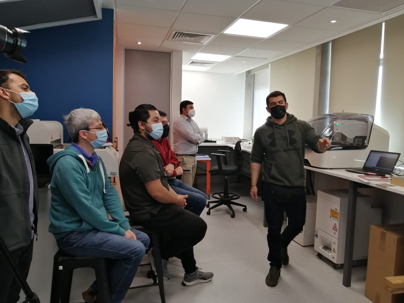
Along that line, the PCB laboratory stands out, as that’s where printed circuit boards, which are the heart of electronic or electrical devices, are produced. “The PCB lab is the place where ideas designed in a CAD environment, in our case Altium Designer, materialize through plating, milling and screen printing until they reach a printed circuit, all locally,” AC3E Labs coordinator Rodrigo Lanas said.
To make better use of the laboratory’s high-tech equipment, the Center provided training to members of the Development Unit, with the participation of senior researcher Pablo Lezana. The five-day course was taught by engineer Oscar Pomar, who is certified in LPKF equipment.
It is expected that this technology and knowledge can also be used for teaching and training AC3E students and possibly be used at other educational institutions.


